Utility Kicad scripts
Making RFID readers and tags requires designing antenna inductors. This tool simplifies the process by allowing you to quickly analyze PCB spiral inductors with FastHenry to find inductance and Q. Once you're satisfied with a design, you can save a Kicad footprint to incorporate into your PCB layout.
You can use it online at http://ignamv2.linkpc.net/spiral/
For local use, download the folder rfid_calculator and run cmdline.py. Example:
$ python3 cmdline.py --help
usage: cmdline.py [-h] --width WIDTH --height HEIGHT --trace_width TRACE_WIDTH
                  [--mirror] --turns TURNS
                  (--pitch PITCH | --separation SEPARATION) [--zpitch ZPITCH]
                  [--frequency FREQUENCY]
                  [--thickness THICKNESS | --weight WEIGHT] [--fasthenry]
                  [--kicad_mod KICAD_MOD] [--pad_size PAD_SIZE]
                  (--mm | --cm | --mil | --in) [--square | --ellipse]
                  [--vertices_per_turn VERTICES_PER_TURN]

Calculate PCB spiral inductor with FastHenry and produce Kicad footprint

optional arguments:
  -h, --help            show this help message and exit
  --width WIDTH         Total outside width
  --height HEIGHT       Total outside height
  --trace_width TRACE_WIDTH
                        Trace width
  --mirror              Reflect footprint horizontally
  --turns TURNS         Number of turns
  --pitch PITCH         Trace pitch (width + separation)
  --separation SEPARATION
                        Separation between traces
  --zpitch ZPITCH       Vertical pitch (default 0 for planar inductor)
  --frequency FREQUENCY
                        Operating frequency
  --thickness THICKNESS
                        Copper thickness
  --weight WEIGHT       Copper weight per unit area in oz/ft²
  --fasthenry           Calculate inductance and Q with FastHenry (
                        http://www.fastfieldsolvers.com )
  --kicad_mod KICAD_MOD
                        Save Kicad footprint to this file
  --pad_size PAD_SIZE   Save Kicad footprint to this file
  --mm                  Dimensions in millimeters
  --cm                  Dimensions in centimeters
  --mil                 Dimensions in mils = 1in / 1000
  --in                  Dimensions in inches
  --square              Generate square spiral
  --ellipse             Generate elliptical spiral
  --vertices_per_turn VERTICES_PER_TURN
                        Number of vertices per turn (for elliptical spirals)

$ python3 cmdline.py --mm --width=50 --height=25 --pitch=5 --trace_width=2 --turns=3 --fasthenry --kicad_mod=/tmp/ant.kicad_mod --frequency=125e3
Analysis of 50.0 mm x 25.0 mm 3-turn 5.0 mm pitch 2.0 mm trace inductor at 125.0 kHz

          Inductance: 11.9 nH
Resonant capacitance: 136.8 µF
                   Q: 5.4e+02

Footprint written to /tmp/ant.kicad_mod
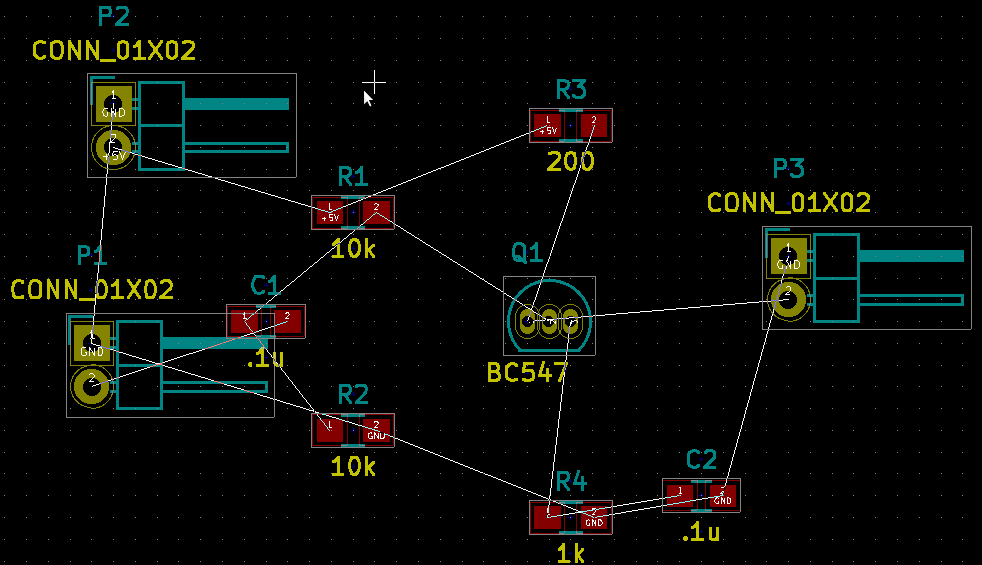
When you first start pcbnew and read a netlist, all components are piled up in one place. This script takes the schematic and pcb files and moves the footprints to match their placement in the schematic. This is a nicer starting point to route your PCB.
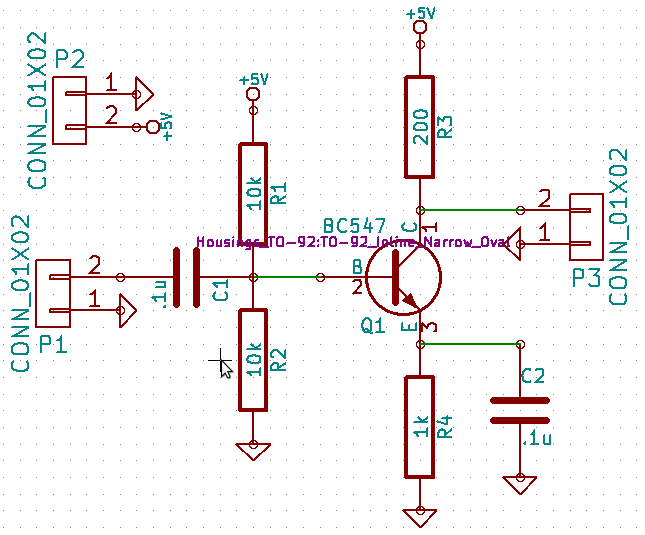
You need to have python 2 installed. First, finish the schematic:
Then export the netlist for pcbnew, and run cvpcb to associate a footprint to each component. Launch pcbnew and load the netlist and footprint association, then save. These are standard steps when making PCBs with Kicad, you can check out Contextual Electronics for more detailed instructions.
My script takes the pcb file you just saved and moves the footprints to match the schematic. You need to download the script to your project directory. To run it, just drag the project file (.pro) or project folder into the script icon. Your pcb file now has placed components.
Here's the output from the schematic above:
If you want to see detailed script output (for troubleshooting), open a terminal (in Windows, use Start -> Run -> cmd.exe) and go to your project directory
$ cd %USERPROFILE%\My Documents\example_project
$ python place_footprints.py .
Found project ./example_project
Found schematic: ././example_project.sch
Found pcb: ././example_project.kicad_pcb
13:06:04: Debug: Skipping general section token 'links'
13:06:04: Debug: Skipping general section token 'area'
13:06:04: Debug: Skipping general section token 'drawings'
13:06:04: Debug: Skipping general section token 'tracks'
13:06:04: Debug: Skipping general section token 'zones'
13:06:04: Debug: Skipping general section token 'symbol'
Moving module...R1 R2 Q1 R4 C2 R3 C1 P1 P3 P2
Backing up ././example_project.kicad_pcb to ././example_project.kicad_pcb.bak6


