32-bit Processor Design
Zaman Ishtiyaq | 15CS01043 | Autumn Semester 2017
Contents
| 1. General purpose registers | 32 |
|---|---|
| 1. Clock cycles per instruction | 4 |
| 1. Instructions | 8 |
| 1. Memory | R.A.M (18-bit Address &32-bit Data) |
| 1. Special Registers | RA, RB, RC, RZ, RY |
OOO AAAAA BBBBB XXXXXXXXXXXXXXXXXXX
| OOO | OP-CODE |
|---|---|
| AAAAA | RA |
| BBBBB | RB |
| XXXXXXXXXXXXXXXXXXX | IMMEDIATE |
| OP-Code | Instruction | RTN |
|---|---|---|
| 000 | LOAD RA, RB, IMMEDIATE | RB [ [RA]+IMMEDIATE ] |
| 001 | STORE* RA, RB, IMMEDIATE | [RB] [ [RA] +IMMEDIATE] |
| 010 | MOV RA, RB | RB [RA] |
| 011 | JUMP RA, RB, IMMEDIATE | PC IMMEDIATE |
| 100 | ADD RA, RB | RB [RA] + [RB] |
| 101 | SUBTRACT RA, RB | RB [RA] - [RB] |
| 110 | MULTIPLY RA, RB | RB [RA] * [RB] |
| 111 | DIVIDE RA, RB | RB [RA] / [RB] |
* STORE can only write to the RAM so the IMMEDTIATE value should be of the form 1XXXXXXXXXXXXXXXXXX as Chip-Select has to select RAM otherwise it will try to write on to the ROM and it will have no effect.
Following are the components along with their figures:
-
-
Fetch Unit:
Fetch Unit increments the PC or jumps to a new address (Immediate Value) when JUMP command is given.
-
Instruction Register and Instruction Decoder:
-
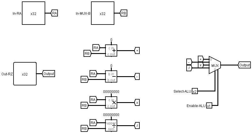
ALU:
Supports Addition, Subtraction, Multiplication and Division.

-
ROM-RAM:
We write our programs on ROM. ROM and RAM are selected based on Chip Select which changes on different operations.
Let us perform the following example:
Initially:
-
Press the RED
-
Change the Register Values in RF to:
R0: 1 R1: 3 R2: 7 R3: 6 R4: 2 R5: 1 R6: 2
-
Let’s Load the ROM with the following values:
00000 : 46280000
00001 : 80080000
00002 : a3200000
00003 : c3280000
00004 : e5080000
00005 : 0008000a
00006 : 202c0000
00007 : 6000000f
00008 : 00000000
.
.
.
0000b : 00000011
.
.
.
0000f : 80080000
00010 : 80080000
When Executed following happens:
R0: 1 R1: 3 R2: 7 R3: 6 R4: 2 R5: 1 R6: 2
-
Stage – 1: Fetch to IR
-
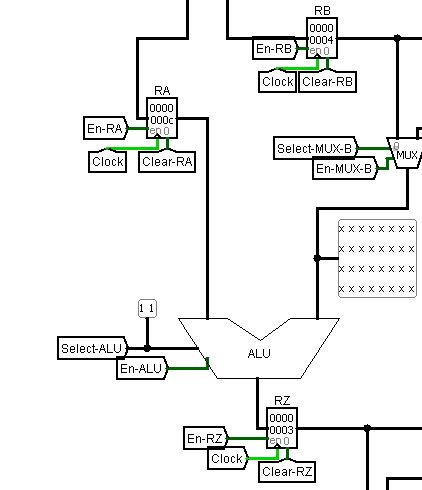
Stage – 2: RA gets value from R6
-
Stage – 3: RA gets value from R6
RA’s value passes unchanged through ALU to RZ
-
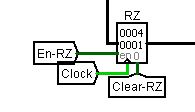
Stage – 4: RY gets value from RZ
-
Stage – 5: R5 gets value from RZ
Values Now:
R0: 1 R1: 3 R2: 7 R3: 6 R4: 2 R5: 2 R6: 2
And PC is incremented to next instruction :
-
80080000 in binary is 100 00000 00001 0000000000000000000
i.e. ADD R0, R1 or R1 [R0] + [R1]
-
Stage – 1: Fetch to IR
-
Stage – 2: RA, RB get their values from RF
-
Stage – 3: ALU performs addition
-
Stage – 4: RY gets value from RZ
-
Stage -5: R1 gets value from RY and PC++
i.e. R1 1 + 3 (=4)
Values Now:
R0: 1 R1: 4 R2: 7 R3: 6 R4: 2 R5: 2 R6: 2
-
a3200000 in binary is 101 00011 00010 0000000000000000000
i.e. SUB R3, R4 or R4 [R3] - [R4]
-
Stage – 1: Fetch to IR
-
Stage – 2: RA, RB get their values from RF
-
Stage – 3: ALU performs Subtraction
-
Stage – 4: RY gets value from RZ
-
Stage -5: R4 gets value from RY and PC++
i.e. R4 6 - 2 (=4)
Values Now:
R0: 1 R1: 4 R2: 7 R3: 6 R4: 4 R5: 2 R6: 2
-
c3280000 in binary is 110 00011 00101 0000000000000000000
i.e. MUL R3, R5 or R5 [R3] * [R5]
-
Stage – 1: Fetch to IR
-
Stage – 2: RA, RB get their values from RF
-
Stage – 3: ALU performs Multiplication
-
Stage – 4: RY gets value from RZ
-
Stage -5: R5 gets value from RY and PC++
i.e. R5 6 * 2 (=12)
Values Now:
R0: 1 R1: 4 R2: 7 R3: 6 R4: 4 R5: 12 R6: 2
-
e5080000 in binary is 111 00101 00001 0000000000000000000
i.e. DIVIDE R5, R1 or R1 [R5] / [R1]
-
Stage – 1: Fetch to IR
-
Stage – 2: RA, RB get their values from RF
-
Stage – 3: ALU performs Division
-
Stage – 4: RY gets value from RZ
-
Stage -5: R1 gets value from RY and PC++
i.e. R5 12 / 4 (=3)
Values Now:
R0: 1 R1: 3 R2: 7 R3: 6 R4: 4 R5: 12 R6: 2
-
0008000a in binary is 000 00000 00001 0000000000000001010
i.e. LOAD R0, R1, #10 or R1 [ [R0] + 10 ]
-
Stage – 2: RA get their values from RF, RB gets IMMEDIATE value
-
Stage – 3: ALU performs Addition, RY gets the address to be read from
-
Stage – 4: RY gets value from the ROM/RAM at address in RY
-
Stage -5: R0 gets value from RY and PC++
i.e. R0 [ [1 + 10] ] which is 0000b location on ROM and the value there is
Values Now R0: 1 R1: 17 R2: 7 R3: 6 R4: 4 R5: 12 R6: 2
-
202c0000 in binary is 001 00000 00010 1000000000000000000
i.e. STORE R0, R5, #0 or [R0] + 0 [R5] i.e. RAM gets written at this location by [R5]
-
Stage – 2: RA get their values from RF, RB gets IMMEDIATE value
-
**Stage – 3: ALU performs Addition, RY gets the address to be write onto, RM gets value of R5
** -
Stage – 4: Value of RM is written on the address in RY
-
6000000f in binary is 011 00000 00000 00000000000000001111
i.e. JUMP IMMEDIATE or PC location 0000f on ROM
-
Stage – 1: Fetch to IR
-
Stage – 2: -
-
**Stage – 3: MUX-PCSet is Enabled and IMMEDIATE is Selected
** -
Stage – 4: PC gets value of IMMEDIATE
-
Now the further instructions are executed from this point onwards.


