The AHA363 is a PCI-Express card intended to perform gzip offload. Since it is cheaply available, and contains an Arria GX FPGA connected to a x4 PCI-Express 2.0 edge connector, this project aims to repurpose it as a general-purpose FPGA development board by reversing and documenting the board itself.
- Reversing of flash format
- JTAG chain access
- 'flashing LED' demo project
- Better understand U6/U7 PSU configuration
- PCIe demo project
- Work out where D3 goes
- Program FPGA via PCIe?
On the PCB are the following devices:
| Designator | Part number | Notes | Datasheet |
|---|---|---|---|
| U1 | AHA3610B | GZip compression ASIC | |
| U2 | AHA3610B | GZip compression ASIC | |
| U3 | Altera EP1AGX90EF1152C6N | The Arria GX FPGA | Handbook |
| U4 | Altera EPM570F100C4N | Altera MAX II CPLD | Handbook |
| U5 | Spansion S29GL128P | 128 MBit Flash IC | Datasheet |
| U6 | Intel EN5365QI | 6A DC-DC converter set to 3.2v (see notes) | Datasheet |
| U7 | Intel EN5365QI | 6A DC-DC converter set to 1.2v (see notes) | Datasheet |
| U8 | Intel EN5365QI | 6A DC-DC converter set to 2.5v | Datasheet |
| U9 | TI LP2996A | DDR Termination regulator (1.5A set to 1.27v) | Datasheet |
| U10 | VPOL5A-12-SMT | 5V DC-DC converter | Datasheet |
| U11 | LM83CIMQA | Temperature sensor | Datasheet |
| U12 | Unknown transistor | Controls D4 | |
| U14 | Intel EN5335QI | 3A DC-DC converter set to 3.3v | Datasheet |
| Y1 | 100MHz clock oscillator | ||
| Y2 | 100MHz clock oscillator | ||
| JP2 | Generic three-pin 1.27inch connector | 12V power input | |
| J2 | 1.27inch PCB edge connector | JTAG | |
| J1 | Unknown | Unknown |
You'll need a toolchain to develop for the device (Quartus), and a means of programming the device, which can be either Quartus, OpenOCD, or some other JTAG programmer. I use a USB 'byte blaster' programmer which works well.
If you're using the free version of Quartus, you'll need to use version 11.0sp1 or older in order to get support for the Arria GX family. Installing this on an older Linux system can require a few tweaks. On my Ubuntu Buster and Xenial boxes, I did the following successfully:
apt-get install -y csh
dpkg --add-architecture i386
apt-get update
apt-get install -y libc6:i386 libsm6:i386 zlib1g:i386 libxrender1:i386 libfreetype6:i386 libfontconfig1:i386 libxext6:i386

curl <location of quartus.tar> -o quartus.tar
tar -xf quartus.tar-C /tmp/quartusinstaller
cd quartus
/tmp/quartusinstaller/quartus_free/install --all --auto /opt/altera
<wait for installer to finish>

# Quartus ships with these two libraries but they don't work properly on a modern ubuntu system. We delete them so that quartus
# will instead use the system versions.
rm /opt/altera/quartus/linux/libX11.so.6 /opt/altera/quartus/linux/libuuid.so.1
If, while trying to launch the installer, you see the following:
`ImportError: /usr/lib/i386-linux-gnu/libfreetype.so.6: symbol png_set_expand_gray_1_2_4_to_8, version PNG12_0 not defined in file libpng12.so.0 with link time reference`
Then you should remove the libpng12.so.0 file from the installer, so that the (newer, function) version on the system is used:
mv altera_installer/bin/libpng12.so.0 ../
bash ./setup
Once you have Quartus successfully installed, you'll need to append to PATH and LD_LIBRARY_PATH to run it:
PATH=$PATH:/opt/altera/quartus/linux/ LD_LIBRARY_PATH=/opt/altera/quartus/linux/ /opt/altera/quartus/linux/quartus
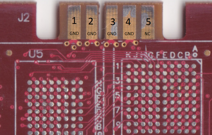
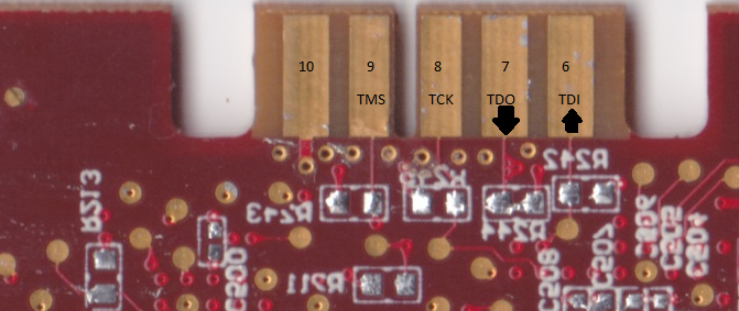
The next step is programming the board. This can be done via the JTAG header, J2, which is a ten-pin edge connector which exposes the CPLD, FPGA, and the two ASICs. The pinout, starting component-side nearest to the PCI bracket:
| Pin | Bottom | Top |
|---|---|---|
| 1 | TDI | NC |
| 2 | TDO | GND |
| 3 | TCK | GND |
| 4 | TMS | GND |
| 5 | VREF (3.3v) | GND |
Or more visually:
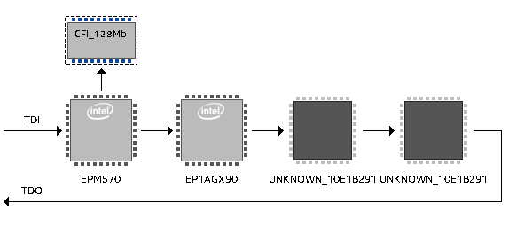
If everything works OK, the chain should scan as follows:
Unfortunately for us, the FPGA also has connections to the JTAG chain via some of its general-purpose IO pins, in addition to the usual JTAG pins. This is probably to facillitate in-sytem programming and/or debugging. If you're using the card in a PCIe slot, this shouldn't be a problem, since the factory gateware will tristate these connections. In your own designs, though, you'll need to be careful to tristate them, otherwise they will interfere with the operation of the JTAG chain:
| FPGA pin | Connection |
|---|---|
| AK14 | TDI on U2 / TDO on FPGA |
| AM23 | TDI of U1 / TDO on U2 |
| AP23 | TDI on CPLD / JTAG connector J2 |
| AN23 | TMS |
| AM22 | TCK |
On power-up, the MAXII CPLD will program the FPGA using a configuration stored in the flash chip U5, and illuminate D4 on success.
- Oscillators Y1 is a 100Mhz oscillator. It connects to pin AJ19 on the FPGA. Y2 is another identical 100MHz oscillator. It connects to Y2 on the FPGA, and also to pin E1 of the CPLD.
- LEDs There are six LEDs on the board. They are numbered D1 to D6, as you'd expect, but they are not laid out sequentially - take care to look at the silkscreen to identify them. D1 is nearest the PCIe backplane connector, and next to it is D2, D3, D5, D6, and finally D4. Four of them connect to the FPGA, one to the CPLD, and one is as-yet unidentified:
| Pin | Purpose |
|---|---|
| AM22 (TCK) | LED_1 |
| AM21 | LED_2 |
| unknown | LED_3 |
| D8 (on the CPLD) | LED_4 |
| AJ21 | LED_5 |
| AL21 | LED_6 |
Note that LED_1 is connected to the JTAG chain, and so using it may disrupt JTAG functionality.
- PCIe The all-important PCIe connector attaches directly to the FPGA.
| Pin | Purpose |
|---|---|
| V2 | REFCLKn |
| V1 | REFCLKp |
| AB5 | HSIn(3) |
| AB4 | HSIp(3) |
| Y5 | HSIn(2) |
| Y4 | HSIp(2) |
| N5 | HSIn(1) |
| N4 | HSIp(1) |
| R5 | HSIn(0) |
| R4 | HSIp(0) |
| AB2 | HSOn(3) |
| AB1 | HSOp(3) |
| Y2 | HSOn(2) |
| Y1 | HSOp(2) |
| N2 | HSOn(1) |
| N1 | HSOp(1) |
| R2 | HSOn(0) |
| R1 | HSOp(0) |
| AJ23 | SMCLK |
| AK23 | SMDATA |
| AL24 | POWERGD |
The board runs from a 12V DC supply, usually from the PCIe edge connector. Alternatively, power can be supplied via JP2, but this can cause problems with the JTAG configuration (see above).
This 12VDC input is converted by U10 (a VPOL5A-12-SMT) into 5VDC, and then this 5V is fed into the following:
| IC | Part | Current output | Notes |
|---|---|---|---|
| U6 | EN5365QI | 6A | configured for 3.3v output |
| U7 | EN5365QI | 6A | configured for 1.2v output |
| U8 | EN5365QI | 6A | configured for 2.5v output |
| U14 | EN5335QI | 3A | configured for 3.3v output |
Note, however, the outputs of U6 and U7 have been bridged. The cause of this is unclear. It is possible that this is a design fault or that U6 and U7 are running in parallel via the MS pin.
If you wish to dump the flash chip which the CPLD uses to configure the FPGA on power-on, this can be done either via Quartus or OpenOCD. Either way, you'll need the card inserted into a powered-on PCI-Express slot, otherwise the JTAG chain may not work correctly (see above).
You can also erase the flash file (or even the CPLD), but be aware that if you do so, the FPGA will not be configured on the next power-up, which may mean you are unable to access JTAG. In this eventuality, you may have to solder wires to the CPLD's TDI and TDO pins directly in order to program the flash.
To dump via Quartus:
- Select 'Hardware Setup', choose the 'USB Blaster' (or whichever programmer you use)
- Click the 'Auto Detect' button. Note that the detection may take a minute or two and appear to hang.
- Select 'CFG_128Mb' and tick the 'Examine' checkbox.
- Hit the 'Start' button to start the dump. It may take a few minutes for the dump to complete.
- Finally, right-click on untitled1.pof and select 'Save File'.
To dump via OpenOCD, tcl scripts are provided in the 'openocd' directory:
sudo /opt/openocd/bin/openocd -f /opt/openocd/share/openocd/scripts/interface/altera-usb-blaster.cfg -f ./aha363.tcl
telnet localhost 4444
source bscan.tcl
- The AHA363 board
- Altera EP1AGX90EF1152C6N: Arria GX 90E
- Altera EPM570F100C4N MAX II CPLD
- MAX II Handbook
- See Arria GX Development Board Reference Manual for 4x PCIe reference design with EPM570 to handle bootup and flash programming.
- Parallel Flash Load IP Core User Guide
- BSDL files for MAX II CPLDs
- BSDL file for EPM570F100


